

Maximum of 25 job preferences reached.
Top Tech Jobs & Startup Jobs

Internet of Things • Semiconductor • Manufacturing
Lead MEMS projects from concept to production, manage timelines and budgets, mitigate risks, and ensure project documentation accuracy.
Top Skills:
Crm SystemsErpMicrosoft ProjectPsa
Internet of Things • Semiconductor • Manufacturing
Recruiter responsible for full-cycle hiring, including sourcing, screening, interviewing, offers, and onboarding. Partners with hiring managers to attract talent, improves candidate experience and employer brand, maintains ATS data and recruiting metrics, and supports HR activities such as onboarding, offboarding, leave administration, and exit interviews. The role is onsite in Goleta, California and requires success in a fast-paced environment.
Top Skills:
Applicant Tracking Systems (Ats)GreenhouseMems Technology
Internet of Things • Semiconductor • Manufacturing
Provides engineering oversight for MEMS foundry process control and production lines. Develops and monitors wafer fabrication processes, operates metrology and fabrication systems, performs root cause analysis, analyzes process performance and yield, applies SPC, optimizes manufacturing processes, maintains technical documentation, and collaborates with fab operations, engineers, technicians, and leadership to ensure quality and production targets.
Top Skills:
ElectroplatingLabviewLean Six SigmaLithographyMetrologyPythonSemiconductor FabricationStatistical Process Control (Spc)Vacuum SystemsWafer-Level TestingWet EtchingYield Analysis
Internet of Things • Semiconductor • Manufacturing
Develops and sustains wafer-level bonding, alignment, etching, electroplating, CMP, grinding, and dicing processes for MEMS fabrication. Improves yield, reduces defects, optimizes process stability, performs DOE and root cause analysis, monitors SPC, and supports equipment qualification and uptime. Collaborates with process engineering, integration, R&D, production, and quality teams in a cleanroom manufacturing environment.
Top Skills:
Chemical Mechanical Polishing (Cmp)Cleanroom ManufacturingDesign Of Experiments (Doe)ElectroplatingMems FabricationSemiconductor FabricationStatistical Process Control (Spc)Wafer BondingWafer DicingWafer GrindingWafer ThinningWet Etching
Internet of Things • Semiconductor • Manufacturing
Develops and supports photolithography processes for MEMS and semiconductor applications. Responsibilities include photomask design using L-Edit, process and tool monitoring, yield and Cpk improvement, equipment qualification, troubleshooting, DOE-based process characterization, recipe standardization, and cross-functional collaboration. The role requires hands-on experience with mask aligners, steppers, automated coat tracks, and strong knowledge of MEMS or semiconductor photolithography.
Top Skills:
Automated Coat TracksCpk AnalysisDesign Of Experiments (Doe)KlayoutL-EditMask AlignersMemsSemiconductor PhotolithographySolidworksStatistical Process Control (Spc)SteppersVlsi Design
New
Track Smarter, Apply Better.
Ditch the spreadsheets. Organize your job search with our freeApplication Tracker.
Use For Free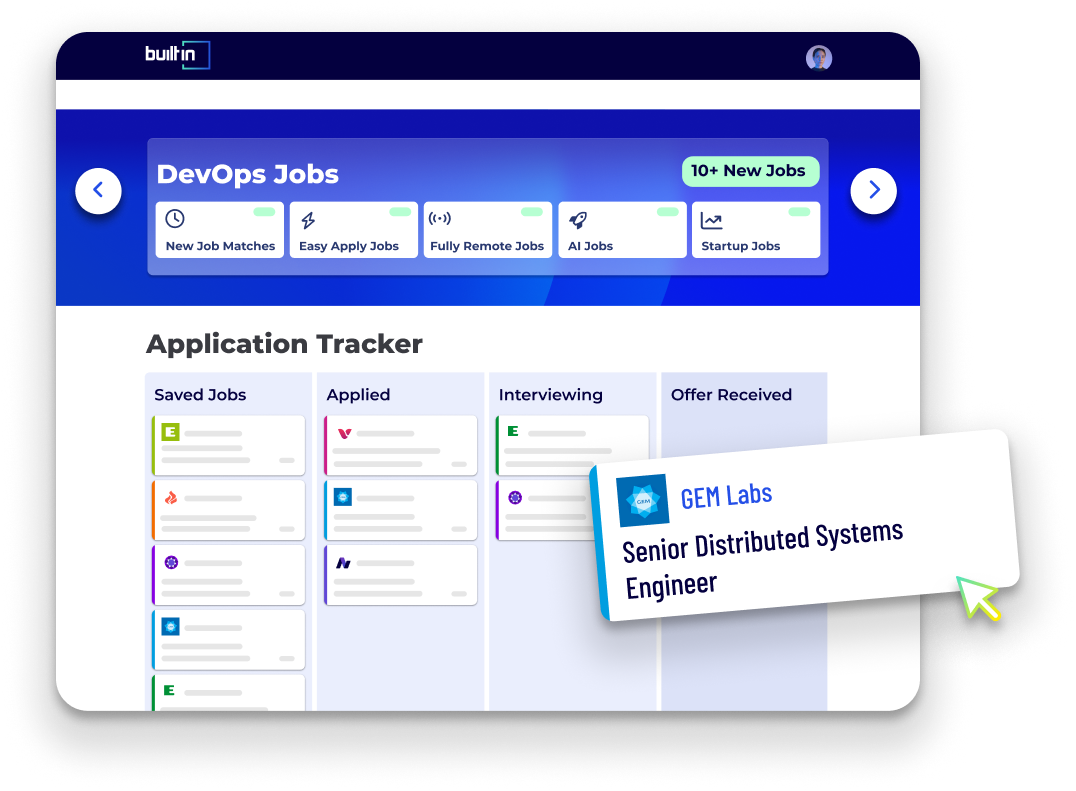
Internet of Things • Semiconductor • Manufacturing
Develops and optimizes high-yield photolithography processes for semiconductor and MEMS manufacturing. Responsibilities include SPC monitoring, Cpk improvement, process and tool troubleshooting, equipment qualification and matching, DOE-based process characterization, recipe standardization, supplier management, manufacturing efficiency improvements, data analysis, and technician mentoring. The role requires hands-on cleanroom work with steppers, contact aligners, photoresist systems, developer tracks, and integration with MES and automation systems.
Top Skills:
Canon SteppersCmosCpkDeveloper SystemsDoeJmpLean Six SigmaMemsMesNikon SteppersPhotolithographyPhotoresist CoatingSemiconductor LithographySpcTel Tracks
Internet of Things • Semiconductor • Manufacturing
The Senior Process Engineer will develop and optimize processes for thin-film applications, troubleshoot production issues, and standardize operations, focusing on deposition techniques and equipment qualifications.
Top Skills:
AldAnnealingBosch ProcessCvdDcDielectric EtchingHdpcvdIon Beam DepositionIon Beam EtchingJmpLpcvdOxidation FurnacesPecvdPlasma AshingPulsed Dc Magnetron SputteringPvdRfRtaRtp
Internet of Things • Semiconductor • Manufacturing
As an Account Development Representative, you will qualify leads, build relationships, and coordinate sales opportunities while learning about the tech industry.
Top Skills:
LinkedInSalesforce
Internet of Things • Semiconductor • Manufacturing
Develop and optimize wafer fabrication processes, lead device development, troubleshoot challenges, and improve manufacturing efficiency in MEMS and photonics technologies.
Top Skills:
C++CmosComsolJavaMemsPythonSemiconductor Fab Tools
Internet of Things • Semiconductor • Manufacturing
The Process Integration Engineer develops MEMS processes, optimizes fabrication, collaborates with teams, and leads technical programs to enhance quality and efficiency.
Top Skills:
ComsolElectroplatingJmpLithographyMemsSpcVacuum SystemsWafer FabricationWet Etch Systems

Let Your Resume Do The Work
Upload your resume to be matched with jobs you're a great fit for.
Success! We'll use this to further personalize your experience.


Popular Job Searches
Tech Jobs & Startup Jobs
Hybrid Jobs
Remote Tech Jobs
.NET Developer Jobs
Account Executive (AE) Jobs
Account Manager (AM) Jobs
Accountant Jobs
Accounting Manager Jobs
Administrative Assistant Jobs
Aerospace Thermal Engineering Jobs
AI Engineer Jobs
Analysis Reporting Jobs
Analytics Jobs
Android Developer Jobs
Application Security Engineer Jobs
Art Director Jobs
Artificial Intelligence Jobs
Assistant Controller Jobs
Associate Product Manager Jobs
Automation Engineer Jobs
Backend Developer Jobs
Blockchain Developer Jobs
Brand Manager Jobs
Business Analyst Jobs
Business Development Manager Jobs
Business Intelligence Jobs
Business Systems Analyst Jobs
C# Jobs
C++ Jobs
Chief of Staff Jobs
Chief Operating Officer Jobs
Cloud Architect Jobs
Cloud Engineer Jobs
Cloud Security Engineer Jobs
Communications Specialist Jobs
Community Manager Jobs
Compliance Analyst Jobs
Content Creator Jobs
Content Jobs
Content Manager Jobs
Content Writer Jobs
Controller Jobs
Copywriter Jobs
Cost Accountant Jobs
Creative Director Jobs
Customer Service Representative Jobs
Customer Success Jobs
Customer Success Manager Jobs
Cyber Security Analyst Jobs
Cyber Security Engineer Jobs
Cyber Security Jobs
Data & Analytics Jobs
Data Analyst Jobs
Data Engineer Jobs
Data Management Jobs
Data Science Jobs
Database Administrator Jobs
Design Engineer Jobs
Desktop Support Jobs
DevOps Engineer Jobs
DevOps Jobs
DevSecOps Engineer Jobs
Director of Engineering Jobs
Director of IT Jobs
Director of Operations Jobs
Editor Jobs
Electrical Engineering Jobs
Embedded Software Engineer Jobs
Engineering Jobs
Engineering Manager Jobs
Environmental Engineering Jobs
Executive Assistant Jobs
Field Engineer Jobs
Field Service Technician Jobs
Finance Jobs
Finance Manager Jobs
Financial Analyst Jobs
Front End Developer Jobs
Full Stack Developer Jobs
Game Designer Jobs
Game Developer Jobs
General Manager Jobs
GIS Analyst Jobs
Golang Jobs
Graphic Designer Jobs
Hardware Engineer Jobs
HR Jobs
Industrial Engineering Jobs
Instructional Designer Jobs
iOS Developer Jobs
IT Jobs
IT Manager Jobs
IT Support Specialist Jobs
IT Systems Administrator Jobs
Java Developer Jobs
Javascript Jobs
Legal Jobs
Linux Jobs
Linux Systems Administrator Jobs
Machine Learning Engineer Jobs
Machine Learning Jobs
Management Trainee Jobs
Manufacturing Engineer Jobs
Marketing Analyst Jobs
Marketing Assistant Jobs
Marketing Associate Jobs
Marketing Coordinator Jobs
Marketing Jobs
Marketing Manager Jobs
Mechanical Engineering Jobs
Network Administrator Jobs
Network Engineer Jobs
Office Administrator Jobs
Office Coordinator Jobs
Office Manager Jobs
Operations Analyst Jobs
Operations Jobs
Operations Manager Jobs
Payroll Specialist Jobs
PHP Developer Jobs
Process Engineer Jobs
Product Analyst Jobs
Product Designer Jobs
Product Manager Jobs
Product Marketing Manager Jobs
Product Owner Jobs
Program Coordinator Jobs
Program Director Jobs
Program Manager Jobs
Project Coordinator Jobs
Project Engineer Jobs
Project Manager Jobs
Prompt Engineering Jobs
Python Jobs
QA Jobs
Quality Manager Jobs
Receptionist Jobs
Research Associate Jobs
Robotics Engineer Jobs
Ruby on Rails Jobs
Sales Development Representative Jobs
Sales Development Representative Jobs
Sales Engineer Jobs
Sales Jobs
Sales Leadership Jobs
Sales Manager Jobs
Sales Operations Jobs
Sales Representative Jobs
Salesforce Administrator Jobs
Salesforce Developer Jobs
Scala Jobs
Scrum Master Jobs
Security Engineer Jobs
Service Desk Analyst Jobs
Sharepoint Developer Jobs
Site Reliability Engineer Jobs
Social Media Coordinator Jobs
Social Media Manager Jobs
Software Engineer Jobs
Software Engineering Manager Jobs
Solutions Architect Jobs
SQL Developer Jobs
Staff Accountant Jobs
Structural Engineer Jobs
Supply Chain Manager Jobs
Support Engineer Jobs
System Engineer Jobs
Systems Administrator Jobs
Systems Analyst Jobs
Tech Support Jobs
Technical Program Manager Jobs
Technical Support Analyst Jobs
Technical Support Engineer Jobs
Technical Support Representative Jobs
Technical Writer Jobs
Test Engineer Jobs
UX Designer Jobs
Web Designer Jobs
Web Developer Jobs
US Jobs
Tech Jobs & Startup Jobs in Albuquerque, NM
Tech Jobs & Startup Jobs in Ann Arbor, MI
Tech Jobs & Startup Jobs in Atlanta, GA
Tech Jobs & Startup Jobs in Baltimore, MD
Tech Jobs & Startup Jobs in Baton Rouge, LA
Tech Jobs & Startup Jobs in Birmingham, AL
Tech Jobs & Startup Jobs in Boise, ID
Tech Jobs & Startup Jobs in Boston, MA
Tech Jobs & Startup Jobs in Buffalo, NY
Tech Jobs & Startup Jobs in Charleston, SC
Tech Jobs & Startup Jobs in Charlotte, NC
Tech Jobs & Startup Jobs in Chicago, IL
Tech Jobs & Startup Jobs in Cincinnati, OH
Tech Jobs & Startup Jobs in Cleveland, OH
Tech Jobs & Startup Jobs in Columbus, OH
Tech Jobs & Startup Jobs in Dallas, TX
Tech Jobs & Startup Jobs in Dayton, OH
Tech Jobs & Startup Jobs in Denver & Boulder, CO
Tech Jobs & Startup Jobs in Des Moines, IA
Tech Jobs & Startup Jobs in Detroit, MI
Tech Jobs & Startup Jobs in Fayetteville, AR
Tech Jobs & Startup Jobs in Greensboro, NC
Tech Jobs & Startup Jobs in Hampton, VA
Tech Jobs & Startup Jobs in Hartford, CT
Tech Jobs & Startup Jobs in Houston, TX
Tech Jobs & Startup Jobs in Huntsville, AL
Tech Jobs & Startup Jobs in Indianapolis, IN
Tech Jobs & Startup Jobs in Jacksonville, FL
Tech Jobs & Startup Jobs in Kansas City, MO
Tech Jobs & Startup Jobs in Las Vegas, NV
Tech Jobs & Startup Jobs in Lexington, KY
Tech Jobs & Startup Jobs in Lincoln, NE
Tech Jobs & Startup Jobs in Little Rock, AR
Tech Jobs & Startup Jobs in Los Angeles, CA
Tech Jobs & Startup Jobs in Louisville, KY
Tech Jobs & Startup Jobs in Madison, WI
Tech Jobs & Startup Jobs in Memphis, TN
Tech Jobs & Startup Jobs in Miami, FL
Tech Jobs & Startup Jobs in Milwaukee, WI
Tech Jobs & Startup Jobs in Minneapolis, MN
Tech Jobs & Startup Jobs in Nashville, TN
Tech Jobs & Startup Jobs in New Orleans, LA
Tech Jobs & Startup Jobs in New York City, NY
Tech Jobs & Startup Jobs in Ogden, UT
Tech Jobs & Startup Jobs in Oklahoma City, OK
Tech Jobs & Startup Jobs in Omaha, NE
Tech Jobs & Startup Jobs in Orlando, FL
Tech Jobs & Startup Jobs in Palm Bay, FL
Tech Jobs & Startup Jobs in Pensacola, FL
Tech Jobs & Startup Jobs in Peoria, IL
Tech Jobs & Startup Jobs in Philadelphia, PA
Tech Jobs & Startup Jobs in Phoenix, AZ
Tech Jobs & Startup Jobs in Pittsburgh, PA
Tech Jobs & Startup Jobs in Portland, OR
Tech Jobs & Startup Jobs in Portland, ME
Tech Jobs & Startup Jobs in Providence, RI
Tech Jobs & Startup Jobs in Provo, UT
Tech Jobs & Startup Jobs in Raleigh, NC
Tech Jobs & Startup Jobs in Reno, NV
Tech Jobs & Startup Jobs in Richmond, VA
Tech Jobs & Startup Jobs in Rochester, NY
Tech Jobs & Startup Jobs in Sacramento, CA
Tech Jobs & Startup Jobs in Salt Lake City, UT
Tech Jobs & Startup Jobs in San Antonio, TX
Tech Jobs & Startup Jobs in San Diego, CA
Tech Jobs & Startup Jobs in San Francisco, CA
Tech Jobs & Startup Jobs in San Luis Obispo, CA
Tech Jobs & Startup Jobs in Santa Cruz, CA
Tech Jobs & Startup Jobs in Seattle, WA
Tech Jobs & Startup Jobs in Spokane, WA
Tech Jobs & Startup Jobs in St. Louis, MO
Tech Jobs & Startup Jobs in Tallahassee, FL
Tech Jobs & Startup Jobs in Tampa Bay, FL
Tech Jobs & Startup Jobs in Tucson, AZ
Tech Jobs & Startup Jobs in Tulsa, OK
Tech Jobs & Startup Jobs in Washington, DC
Tech Jobs & Startup Jobs in Wichita, KS
Tech Jobs & Startup Jobs in Wilmington, NC
International Jobs
Tech Jobs & Startup Jobs in Bangalore
Tech Jobs & Startup Jobs in Brazil
Tech Jobs & Startup Jobs in Czechia
Tech Jobs & Startup Jobs in Germany
Tech Jobs & Startup Jobs in Hungary
Tech Jobs & Startup Jobs in India
Tech Jobs & Startup Jobs in Israel
Tech Jobs & Startup Jobs in Italy
Tech Jobs & Startup Jobs in Japan
Tech Jobs & Startup Jobs in Malaysia
Tech Jobs & Startup Jobs in Mexico
Tech Jobs & Startup Jobs in Netherlands
Tech Jobs & Startup Jobs in New Zealand
Tech Jobs & Startup Jobs in Poland
Tech Jobs & Startup Jobs in Romania
Tech Jobs & Startup Jobs in Spain
Tech Jobs & Startup Jobs in the Philippines
Tech Jobs & Startup Jobs in Turkey
All Filters
Total selected ()
No Results
No Results
