

Maximum of 25 job preferences reached.
Top Tech Jobs & Startup Jobs

Semiconductor • Manufacturing
Leads global quality programs and the 8D nonconformance-resolution process. Responsibilities include optimizing program execution, analyzing quality and manufacturing data, conducting audits, coaching stakeholders on structured problem-solving, preventing recurrence, improving supplier and product quality, reducing poor-quality costs, and driving quality culture and change management across global sites.
Top Skills:
8DArtificial IntelligenceData AnalyticsDmaicIso 9001:2015Lean Six SigmaPdcaSemiconductor Manufacturing
Semiconductor • Manufacturing
Designs, selects, tests, and documents RF power delivery systems from 100 kHz to 100 MHz and watt to kilowatt power levels. Performs electrical engineering research and development for complex embedded and electromechanical systems, collaborates with multidisciplinary teams and suppliers, develops test plans, analyzes data, troubleshoots systems, and presents findings in design and program reviews. The role supports semiconductor etch and deposition products.
Top Skills:
Ai ToolsComsolCst Microwave StudioElectromagnetic ModelingHfssHigh-Voltage DesignImpedance AnalyzersMathcadMatlabNetwork AnalyzersPower MetersPythonRf Measurement EquipmentRf Power Delivery SystemsSpectrum AnalyzersSpice
Semiconductor • Manufacturing
Develops and supports semiconductor equipment from prototyping through product release and initial field deployment. Designs experiments, tests, and prototypes; analyzes complex technical issues; and provides troubleshooting, repair, and debugging support. Collaborates with customers and cross-functional teams to improve product quality and resolve issues. The role includes cleanroom and semiconductor fab work, customer engagement, and international travel of up to 25%.
Top Skills:
Cleanroom TechnologySemiconductor EquipmentSemiconductor Manufacturing
Semiconductor • Manufacturing
Owns unreleased build plans, DMRFs, refurbished tools, product upgrades, part transitions, material movements, and field missing-part escalations. Supports excess and obsolete inventory reduction, spares transitions, and working capital initiatives. Provides status reporting, risk assessments, and recovery plans while coordinating cross-functional stakeholders and driving process improvements across product operations, manufacturing, and supply chain activities.
Top Skills:
Erp SystemsPlanning SystemsProduct Lifecycle Management Systems
Semiconductor • Manufacturing
Leads technical product and process programs from initiation through release. Develops plans, manages schedules, budgets, risks, and performance metrics, and coordinates cross-functional teams. Partners with stakeholders on system and process enhancements, leads continuous improvement and change management initiatives, performs statistical analysis, and drives sustainable outcomes across multiple projects. The role supports semiconductor product development and requires strong communication, executive presentation, and stakeholder-influence skills.
Top Skills:
AgileLean Six SigmaMs ProjectOffice TimelineQuickbaseWaterfall
New
Track Smarter, Apply Better.
Ditch the spreadsheets. Organize your job search with our freeApplication Tracker.
Use For Free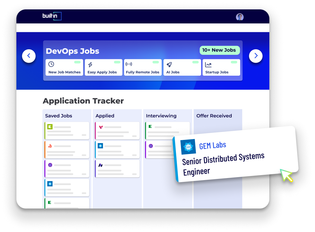
Semiconductor • Manufacturing
Conduct semiconductor process engineering research and development, improve fabrication methods, reduce costs, increase yields, analyze process and test data, and support customer demonstrations and next-generation product releases. The role also defines equipment and process requirements, develops advanced process formulations, applies statistical methods, and provides technical guidance to process technicians.
Top Skills:
Atomic Layer Deposition (Ald)Atomic Layer Etching (Ale)Capacitively Coupled Plasma (Ccp)Chemical Vapor Deposition (Cvd)Design Of Experiments (Doe)Inductively Coupled Plasma (Icp)JmpMaterial CharacterizationMaterial SynthesisMatlabMinitabPhysical Vapor Deposition (Pvd)Plasma Enhanced Chemical Vapor Deposition (Pecvd)Plasma PhysicsPythonReactive Ion Etching (Rie)Semiconductor EquipmentStatistical Process Control (Spc)
3 Days AgoSaved
Semiconductor • Manufacturing
Develop physics-based and machine-learning surrogate models for plasma etch processes and semiconductor feature profiles. Responsibilities include modeling plasma-surface interactions, calibrating simulations against SEM/TEM measurements, designing simulation experiments, validating surrogate models, optimizing process conditions, and automating workflows with Python. The intern will document methods and present results while collaborating with Lam Research’s technical community.
Top Skills:
BotorchFinite Element SimulationGaussian ProcessesGpytorchJaxMonte Carlo SimulationNeural NetworksPolynomial ChaosPythonPyTorchSemTemTensorFlow
Semiconductor • Manufacturing
Develop and improve semiconductor manufacturing processes and equipment applications. The role conducts process research, evaluates test data, applies SPC and DOE, supports customer demonstrations, and contributes to next-generation product development. Responsibilities include defining equipment requirements, improving yield and costs, collaborating with customers and cross-functional teams, guiding process technicians, and introducing new technologies at customer sites.
Top Skills:
Atomic Layer Deposition (Ald)Atomic Layer Etching (Ale)Capacitively Coupled Plasma (Ccp)Chemical Vapor Deposition (Cvd)Design Of Experiments (Doe)Inductively Coupled Plasma (Icp)JmpMaterial CharacterizationMaterial SynthesisMatlabMinitabPhysical Vapor Deposition (Pvd)Plasma Enhanced Chemical Vapor Deposition (Pecvd)Plasma PhysicsPythonReactive Ion Etching (Rie)Semiconductor EquipmentStatistical Process Control (Spc)
Semiconductor • Manufacturing
Develop and implement advanced metrology and diagnostic solutions for semiconductor process control and defect detection. Apply spectroscopy, analytical characterization, machine learning, and deep learning to understand process interactions, model defectivity, and optimize manufacturing processes. Collaborate with process, product, inspection, and simulation teams; evaluate emerging e-beam technologies; and establish SPC-based monitoring and qualification methods for metrology assets. Support low-GWP process technology development and advanced semiconductor manufacturing applications.
Top Skills:
CnnDeep LearningDesign Of Experiments (Doe)E-Beam InspectionFtirGp-FtirMachine LearningMass SpectrometryPythonRaman SpectroscopySemiconductor EquipmentStatistical Process Control (Spc)Uv-VisXpsXrdXrfXrr
Semiconductor • Manufacturing
Develops and optimizes advanced semiconductor etch processes for specialty and advanced packaging applications. Designs and analyzes experiments, establishes process windows, defines hardware requirements, solves complex manufacturing challenges, and supports customer demonstrations. Collaborates with customers and cross-functional teams to introduce new technologies, improve yield and productivity, and transition process innovations from development through production at worldwide customer sites.
Top Skills:
3D IntegrationAdvanced PackagingCapacitively Coupled Plasma (Ccp)Conductor FilmsDeep Silicon EtchDepositionDesign Of Experiments (Doe)Dielectric FilmsFrame-Form Plasma DicingHbmInductively Coupled Plasma (Icp)Materials CharacterizationMetal FilmsPlasma EtchingReactive Ion Etching (Rie)Semiconductor Process DevelopmentStatistical AnalysisTsvWafer Handling Systems

Let Your Resume Do The Work
Upload your resume to be matched with jobs you're a great fit for.
Success! We'll use this to further personalize your experience.
Top Companies Hiring
See All

Popular Job Searches
Tech Jobs & Startup Jobs
Hybrid Jobs
Remote Tech Jobs
.NET Developer Jobs
Account Executive (AE) Jobs
Account Manager (AM) Jobs
Accountant Jobs
Accounting Manager Jobs
Administrative Assistant Jobs
Aerospace Thermal Engineering Jobs
AI Engineer Jobs
Analysis Reporting Jobs
Analytics Jobs
Android Developer Jobs
Application Security Engineer Jobs
Art Director Jobs
Artificial Intelligence Jobs
Assistant Controller Jobs
Associate Product Manager Jobs
Automation Engineer Jobs
Backend Developer Jobs
Blockchain Developer Jobs
Brand Manager Jobs
Business Analyst Jobs
Business Development Manager Jobs
Business Intelligence Jobs
Business Systems Analyst Jobs
C# Jobs
C++ Jobs
Chief of Staff Jobs
Chief Operating Officer Jobs
Cloud Architect Jobs
Cloud Engineer Jobs
Cloud Security Engineer Jobs
Communications Specialist Jobs
Community Manager Jobs
Compliance Analyst Jobs
Content Creator Jobs
Content Jobs
Content Manager Jobs
Content Writer Jobs
Controller Jobs
Copywriter Jobs
Cost Accountant Jobs
Creative Director Jobs
Customer Service Representative Jobs
Customer Success Jobs
Customer Success Manager Jobs
Cyber Security Analyst Jobs
Cyber Security Engineer Jobs
Cyber Security Jobs
Data & Analytics Jobs
Data Analyst Jobs
Data Engineer Jobs
Data Management Jobs
Data Science Jobs
Database Administrator Jobs
Design Engineer Jobs
Desktop Support Jobs
DevOps Engineer Jobs
DevOps Jobs
DevSecOps Engineer Jobs
Director of Engineering Jobs
Director of IT Jobs
Director of Operations Jobs
Editor Jobs
Electrical Engineering Jobs
Embedded Software Engineer Jobs
Engineering Jobs
Engineering Manager Jobs
Environmental Engineering Jobs
Executive Assistant Jobs
Field Engineer Jobs
Field Service Technician Jobs
Finance Jobs
Finance Manager Jobs
Financial Analyst Jobs
Front End Developer Jobs
Full Stack Developer Jobs
Game Designer Jobs
Game Developer Jobs
General Manager Jobs
GIS Analyst Jobs
Golang Jobs
Graphic Designer Jobs
Hardware Engineer Jobs
HR Jobs
Industrial Engineering Jobs
Instructional Designer Jobs
iOS Developer Jobs
IT Jobs
IT Manager Jobs
IT Support Specialist Jobs
IT Systems Administrator Jobs
Java Developer Jobs
Javascript Jobs
Legal Jobs
Linux Jobs
Linux Systems Administrator Jobs
Machine Learning Engineer Jobs
Machine Learning Jobs
Management Trainee Jobs
Manufacturing Engineer Jobs
Marketing Analyst Jobs
Marketing Assistant Jobs
Marketing Associate Jobs
Marketing Coordinator Jobs
Marketing Jobs
Marketing Manager Jobs
Mechanical Engineering Jobs
Network Administrator Jobs
Network Engineer Jobs
Office Administrator Jobs
Office Coordinator Jobs
Office Manager Jobs
Operations Analyst Jobs
Operations Jobs
Operations Manager Jobs
Payroll Specialist Jobs
PHP Developer Jobs
Process Engineer Jobs
Product Analyst Jobs
Product Designer Jobs
Product Manager Jobs
Product Marketing Manager Jobs
Product Owner Jobs
Program Coordinator Jobs
Program Director Jobs
Program Manager Jobs
Project Coordinator Jobs
Project Engineer Jobs
Project Manager Jobs
Prompt Engineering Jobs
Python Jobs
QA Jobs
Quality Manager Jobs
Receptionist Jobs
Research Associate Jobs
Robotics Engineer Jobs
Ruby on Rails Jobs
Sales Development Representative Jobs
Sales Development Representative Jobs
Sales Engineer Jobs
Sales Jobs
Sales Leadership Jobs
Sales Manager Jobs
Sales Operations Jobs
Sales Representative Jobs
Salesforce Administrator Jobs
Salesforce Developer Jobs
Scala Jobs
Scrum Master Jobs
Security Engineer Jobs
Service Desk Analyst Jobs
Sharepoint Developer Jobs
Site Reliability Engineer Jobs
Social Media Coordinator Jobs
Social Media Manager Jobs
Software Engineer Jobs
Software Engineering Manager Jobs
Solutions Architect Jobs
SQL Developer Jobs
Staff Accountant Jobs
Structural Engineer Jobs
Supply Chain Manager Jobs
Support Engineer Jobs
System Engineer Jobs
Systems Administrator Jobs
Systems Analyst Jobs
Tech Support Jobs
Technical Program Manager Jobs
Technical Support Analyst Jobs
Technical Support Engineer Jobs
Technical Support Representative Jobs
Technical Writer Jobs
Test Engineer Jobs
UX Designer Jobs
Web Designer Jobs
Web Developer Jobs
US Jobs
Tech Jobs & Startup Jobs in Albuquerque, NM
Tech Jobs & Startup Jobs in Ann Arbor, MI
Tech Jobs & Startup Jobs in Atlanta, GA
Tech Jobs & Startup Jobs in Baltimore, MD
Tech Jobs & Startup Jobs in Baton Rouge, LA
Tech Jobs & Startup Jobs in Birmingham, AL
Tech Jobs & Startup Jobs in Boise, ID
Tech Jobs & Startup Jobs in Boston, MA
Tech Jobs & Startup Jobs in Buffalo, NY
Tech Jobs & Startup Jobs in Charleston, SC
Tech Jobs & Startup Jobs in Charlotte, NC
Tech Jobs & Startup Jobs in Chicago, IL
Tech Jobs & Startup Jobs in Cincinnati, OH
Tech Jobs & Startup Jobs in Cleveland, OH
Tech Jobs & Startup Jobs in Columbus, OH
Tech Jobs & Startup Jobs in Dallas, TX
Tech Jobs & Startup Jobs in Dayton, OH
Tech Jobs & Startup Jobs in Denver & Boulder, CO
Tech Jobs & Startup Jobs in Des Moines, IA
Tech Jobs & Startup Jobs in Detroit, MI
Tech Jobs & Startup Jobs in Fayetteville, AR
Tech Jobs & Startup Jobs in Greensboro, NC
Tech Jobs & Startup Jobs in Hampton, VA
Tech Jobs & Startup Jobs in Hartford, CT
Tech Jobs & Startup Jobs in Houston, TX
Tech Jobs & Startup Jobs in Huntsville, AL
Tech Jobs & Startup Jobs in Indianapolis, IN
Tech Jobs & Startup Jobs in Jacksonville, FL
Tech Jobs & Startup Jobs in Kansas City, MO
Tech Jobs & Startup Jobs in Las Vegas, NV
Tech Jobs & Startup Jobs in Lexington, KY
Tech Jobs & Startup Jobs in Lincoln, NE
Tech Jobs & Startup Jobs in Little Rock, AR
Tech Jobs & Startup Jobs in Los Angeles, CA
Tech Jobs & Startup Jobs in Louisville, KY
Tech Jobs & Startup Jobs in Madison, WI
Tech Jobs & Startup Jobs in Memphis, TN
Tech Jobs & Startup Jobs in Miami, FL
Tech Jobs & Startup Jobs in Milwaukee, WI
Tech Jobs & Startup Jobs in Minneapolis, MN
Tech Jobs & Startup Jobs in Nashville, TN
Tech Jobs & Startup Jobs in New Orleans, LA
Tech Jobs & Startup Jobs in New York City, NY
Tech Jobs & Startup Jobs in Ogden, UT
Tech Jobs & Startup Jobs in Oklahoma City, OK
Tech Jobs & Startup Jobs in Omaha, NE
Tech Jobs & Startup Jobs in Orlando, FL
Tech Jobs & Startup Jobs in Palm Bay, FL
Tech Jobs & Startup Jobs in Pensacola, FL
Tech Jobs & Startup Jobs in Peoria, IL
Tech Jobs & Startup Jobs in Philadelphia, PA
Tech Jobs & Startup Jobs in Phoenix, AZ
Tech Jobs & Startup Jobs in Pittsburgh, PA
Tech Jobs & Startup Jobs in Portland, OR
Tech Jobs & Startup Jobs in Portland, ME
Tech Jobs & Startup Jobs in Providence, RI
Tech Jobs & Startup Jobs in Provo, UT
Tech Jobs & Startup Jobs in Raleigh, NC
Tech Jobs & Startup Jobs in Reno, NV
Tech Jobs & Startup Jobs in Richmond, VA
Tech Jobs & Startup Jobs in Rochester, NY
Tech Jobs & Startup Jobs in Sacramento, CA
Tech Jobs & Startup Jobs in Salt Lake City, UT
Tech Jobs & Startup Jobs in San Antonio, TX
Tech Jobs & Startup Jobs in San Diego, CA
Tech Jobs & Startup Jobs in San Francisco, CA
Tech Jobs & Startup Jobs in San Luis Obispo, CA
Tech Jobs & Startup Jobs in Santa Cruz, CA
Tech Jobs & Startup Jobs in Seattle, WA
Tech Jobs & Startup Jobs in Spokane, WA
Tech Jobs & Startup Jobs in St. Louis, MO
Tech Jobs & Startup Jobs in Tallahassee, FL
Tech Jobs & Startup Jobs in Tampa Bay, FL
Tech Jobs & Startup Jobs in Tucson, AZ
Tech Jobs & Startup Jobs in Tulsa, OK
Tech Jobs & Startup Jobs in Washington, DC
Tech Jobs & Startup Jobs in Wichita, KS
Tech Jobs & Startup Jobs in Wilmington, NC
International Jobs
Tech Jobs & Startup Jobs in Bangalore
Tech Jobs & Startup Jobs in Brazil
Tech Jobs & Startup Jobs in Czechia
Tech Jobs & Startup Jobs in Germany
Tech Jobs & Startup Jobs in Hungary
Tech Jobs & Startup Jobs in India
Tech Jobs & Startup Jobs in Israel
Tech Jobs & Startup Jobs in Italy
Tech Jobs & Startup Jobs in Japan
Tech Jobs & Startup Jobs in Malaysia
Tech Jobs & Startup Jobs in Mexico
Tech Jobs & Startup Jobs in Netherlands
Tech Jobs & Startup Jobs in New Zealand
Tech Jobs & Startup Jobs in Poland
Tech Jobs & Startup Jobs in Romania
Tech Jobs & Startup Jobs in Spain
Tech Jobs & Startup Jobs in the Philippines
Tech Jobs & Startup Jobs in Turkey
All Filters
Total selected ()
No Results
No Results
