Essential Duties:
We are seeking a yield improvement and failure analysis engineer for a high mix and low volume fab.
The individual will work with integration, production, and process engineers to find root cause of device failures, implement process improvement plans, create design of experiment (DOE) using JMP, and report findings to department and program staff.
The engineer will perform materials characterization at HRL and also help coordinate sample analysis at external characterization labs.
Required Skills:
Materials characterization including SEM, FIB, TEM
Cleanroom experience
Understanding of semiconductor processes
The candidate should have 2+ years of experience in yield engineering, device failure analysis, semiconductor process development, wafer fabrication, materials characterization, or data analysis.
The role requires understanding of at least one semiconductor process module (PHOTO, DRY ETCH, WET ETCH, METROLOGY, THIN FILM, CVD, CMP, TEST, and PACKAGING).
The role requires attention to detail and excellent verbal and written communications.
Required Education:
B.S. degree in Electrical Engineering, Physics, Chemistry, Materials Science, or a STEM related field plus 2+ years of work experience or graduate education.
Physical Requirements:
Must be willing to work in a cleanroom (up to 30%)
Special Requirements:
U.S. Citizenship.
Must have or be willing to apply for a security clearance
Compensation:
The base salary range for this full-time position is $132,765 - $165,983 + bonus + benefits.
Our salary ranges are determined by role, level, and location. The range displayed on each job posting reflects the minimum and maximum target for new hire salaries for the position. Within the range, individual pay is determined by work location and additional factors, including job-related skills, experience, and relevant education or training. Your recruiter can share more about the specific salary range during the hiring process. Please note that the compensation details listed reflect the base salary only, and do not include potential bonus or benefits.
What the Team is Saying


What We Do
HRL Laboratories, LLC, Malibu, California, (hrl.com) pioneers the next frontiers of physical and information science. Delivering transformative technologies in automotive, aerospace and defense, HRL advances the critical missions of its customers. As a private company owned jointly by Boeing and GM, HRL is a source of innovations that advance the state of the art in profound and far-reaching ways.
Why Work With Us
Our success is the result of our collaborative team of researchers, many of whom are the leading experts in their fields. Through their insights in support for our customers, we are finding the unique opportunities in technology.
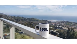
Gallery
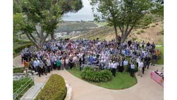


HRL Laboratories Offices
Hybrid Workspace
Employees engage in a combination of remote and on-site work.
Hybrid Policy is role specific.