

Microprocessors are built from transistors, most commonly metal-oxide semiconductor (MOS) transistors.
The two types of MOS transistors are n-type MOS (nMOS) and p-type MOS (pMOS), which differ in structure, behavior and their charge carriers. Both devices have three terminals: gate, source and drain.
What are NMOS Transistors and PMOS Transistors?
- NMOS Transistor: Turns on when the gate voltage is high relative to the source, creating a conductive path between drain and source.
- PMOS Transistor: Turns on when the gate voltage is low relative to the source, also creating a conductive path between drain and source.
To understand how a pMOS and an nMOS operate, you also need to know a couple key terms:
- Closed circuit: Electricity is flowing between the source and the drain, enabling the circuit to conduct.
- Open circuit: Electricity is not flowing between the source and drain, as the path is blocked by transistor.
How Does an NMOS Transistor Work?
When the gate-to-source voltage of an nMOS transistor exceeds its threshold voltage, a conductive channel forms between the drain and source, allowing current to flow. This means the transistor is in a closed-circuit state, or on.
If gate-to-source voltage is below the threshold (e.g., near 0 volts), the channel does not form and no current flows between the drain and source. This means the transistor is in an open-circuit state, or off.

How Does a PMOS Transistor Work?
A pMOS transistor works in the opposite manner of an nMOS transistor. It turns on when the gate voltage is low relative to the source.
On circuit diagrams (like the one below), the pMOS symbol includes a small circle (or “bubble”) at the gate terminal. This bubble signifies that the transistor is active-low — it turns on when receiving a low logic level. As a note, the bubble represents logical inversion, not a literal voltage inversion; it simply indicates the gate responds to opposite logic compared to the nMOS.

Constructing NMOS and PMOS Transistor Gates
Because pMOS and nMOS transistors operate in complementary ways, they can be combined into a complementary metal-oxide semiconductor (cMOS) circuit, and be used to build logic gates.
‘NOT’ Gate With NMOS and PMOS Transistors
Pairing a pMOS connected to the source or supply voltage with an nMOS connected to ground allows us to build logic structures, starting with the simplest example: a NOT gate.
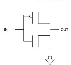
This cMOS transistor acts in a similar manner to the NOT logical function.
A NOT gate can be built using one pMOS transistor at the top and one nMOS transistor at the bottom:
- Input = 0: The pMOS is on, connecting the output to the supply voltage. The nMOS is off, so there is no path to ground. Output = 1.
- Input = 1: The pMOS is off, disconnecting the supply. The nMOS is on, pulling the output down to ground. Output = 0.
This matches the truth table of a NOT gate: the output is always the opposite of the input.
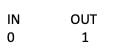
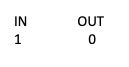
Putting the two sets of input/output together yields:

It’s quite easy to see that this truth table is the exact same as that which the logical function NOT produces:

As a result, this is known as a NOT gate.
Can we use these two simple transistors to make more complicated structures? Absolutely.
‘NOT-OR’ Gate With NMOS and PMOS Transistors
Next, we will build a NOT-OR (NOR) gate.
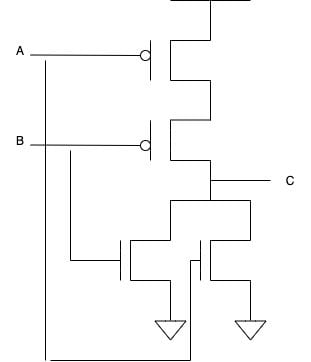
This circuit uses two pMOS transistors at the top and two nMOS transistors at the bottom.
- A = 0, B = 0: Both pMOS conduct, pulling the output high. Both nMOS are off, so no path to ground. Output = 1.
- A = 0, B = 1: The pMOS connected to A is on, but the pMOS connected to B is off. At least one pMOS is off, so the output is not pulled high. The nMOS for B conducts, pulling the output low. Output = 0.
- A = 1, B = 0: Similar to the previous case, one pMOS is off and the corresponding nMOS is on, pulling the output low. Output = 0.
- A = 1, B = 1: Both pMOS are off, so the output isn’t pulled high. Both nMOS are on, pulling the output firmly low. Output = 0.
The above gate’s truth table is as follows:
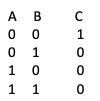
This matches the truth table of a NOR gate: the output is high only when both inputs are 0, and low in all other cases.

Thus, we have confirmed that this gate is a NOR gate because it shares its truth table with the NOR logical function.
‘OR’ Gate With NMOS and PMOS Transistors
Now, we will put both of the gates that we have created together in order to produce an OR gate. Remember, NOR stands for NOT OR. So, if we invert an already inverted gate, we will get the original back.
Let’s put this to the test to see it in action.

The OR gate is constructed by taking the NOR gate and adding an inverter (a NOT gate) to its output.
- A = 0, B = 0: The NOR gate produces 1, but the inverter flips it to 0. Output = 0.
- A = 0, B = 1: The NOR gate produces 0, the inverter flips it to 1. Output = 1.
- A = 1, B = 0: The NOR gate produces 0, the inverter flips it to 1. Output = 1.
- A = 1, B = 1: The NOR gate produces 0, the inverter flips it to 1. Output = 1.
Thus, the truth table will be as follows:

This matches the truth table of an OR gate: the output is high when at least one input is high.
‘NOT-AND’ Gate With NMOS and PMOS Transistors

I claim this is a NOT AND (NAND) gate, but let’s test this gate’s truth table to determine if it really is a NAND gate.
This circuit combines pMOS transistors at the top and nMOS transistors at the bottom.
- A = 0, B = 0: Both pMOS conduct, pulling the output high. Both nMOS are off, so no path to ground. Output = 1.
- A = 0, B = 1: The pMOS for A conducts, pulling the output high. The nMOS for B is on, but since A’s nMOS is off, there’s no full path to ground. Output = 1.
- A = 1, B = 0: The pMOS for B conducts, pulling the output high. The nMOS for A is on, but B’s nMOS is off, so no path to ground. Output = 1.
- A = 1, B = 1: Both pMOS are off, so no pull-up. Both nMOS are on, creating a path to ground. Output = 0.
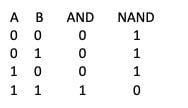
The above gate’s truth table is as follows:

This matches the truth table of a NAND gate: the output is high for all input combinations except when both inputs are 1.

Thus, we have verified that this is, indeed, a NAND gate.
‘AND’ Gate With NMOS and PMOS Transistors
Now we will build an AND gate the exact same way we built an OR gate from a NOR gate. We will attach an inverter.

Since all we have done is applied a NOT function to a NAND gate’s output, the truth table will look like this:
Again, please verify to make sure that what I am telling you is true.
Thus we’ve covered what pMOS and nMOS transistors are, as well as how to use them to build more complex structures.
Frequently Asked Questions
What is a NMOS transistor?
An NMOS (n-type MOS) transistor is a transistor with a metal-oxide semiconductor (MOS) structure, where n-type material is used for the source and the drain terminals and p-type material is used for the substrate.
An NMOS transistor turns on (current flow between source and drain) when the gate-to-source voltage is high enough to exceed its threshold voltage, and turns off (no current) when it receives a voltage around 0 volts or below the threshold.
What is a PMOS transistor?
A PMOS (p-type MOS) transistor is a transistor with a metal-oxide semiconductor (MOS) structure, where p-type material is used for the source and drain terminals and n-type material is used for the substrate.
A PMOS transistor turns on (current flow between source and drain) when the gate-to-source voltage is low relative to the source, and turns off (no current) when the gate voltage is high relative to the source.
What is the difference between NMOS and PMOS transistors?
NMOS transistors have n-type (electron-based) source and drain terminals and a p-type substrate, while PMOS transistors have p-type (hole-based) source and drain terminals and an n-type substrate. NMOS transistors turn on with a high gate voltage, and PMOS transistors turn on with a low gate voltage.

