The Role
OUR STORY
TechInsights is the information Platform for the semiconductor industry.
Regarded as the most trusted source of actionable, in-depth intelligence related to semiconductor innovation and surrounding markets, TechInsights’ content informs decision makers and professionals whose success depends on accurate knowledge of the semiconductor industry—past, present, or future.
Over 650 companies and 150,000 users access the TechInsights Platform, the world’s largest vertically integrated collection of unmatched reverse engineering, teardown, and market analysis in the semiconductor industry. This collection includes detailed circuit analysis, imagery, semiconductor process flows, device teardowns, illustrations, costing and pricing information, forecasts, market analysis, and expert commentary. TechInsights’ customers include the most successful technology companies who rely on TechInsights’ analysis to make informed business, design, and product decisions faster and with greater confidence. For more information, visit www.techinsights.com.
WHY WORK WITH US
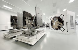
TechInsights' Front-End Teardown Lab is hiring a Teardown Lab Specialist to join our team during the 6:00am - 2:00pm shift. As the successful candidate, you will be responsible for the disassembly of electronic products and capturing high quality optical images and product data of the components. You will safely use chemical and mechanical processes to expose external structures and using professional DSLR cameras and optical microscopes to capture high resolution images for subsequent analysis.
At the developing level, you are an individual contributor with basic skills and knowledge acquired through work experience or education. The Teardown Lab Specialist applies learned skills and knowledge to complete assigned tasks while working autonomously on routine tasks and receives guidance and supervision for moderately complex tasks. The Teardown Lab Specialist learns and uses established practices and standard procedures to complete assignments, and willingly accepts guidance and feedback to improve skills.
WHAT YOU’LL DO
WORKING ARRANGEMENT
This role is on site at our Ottawa office.
TechInsights is the information Platform for the semiconductor industry.
Regarded as the most trusted source of actionable, in-depth intelligence related to semiconductor innovation and surrounding markets, TechInsights’ content informs decision makers and professionals whose success depends on accurate knowledge of the semiconductor industry—past, present, or future.
Over 650 companies and 150,000 users access the TechInsights Platform, the world’s largest vertically integrated collection of unmatched reverse engineering, teardown, and market analysis in the semiconductor industry. This collection includes detailed circuit analysis, imagery, semiconductor process flows, device teardowns, illustrations, costing and pricing information, forecasts, market analysis, and expert commentary. TechInsights’ customers include the most successful technology companies who rely on TechInsights’ analysis to make informed business, design, and product decisions faster and with greater confidence. For more information, visit www.techinsights.com.
WHY WORK WITH US
- Company-sponsored training and development opportunities
- Comprehensive benefits package (health, dental, vision, wellness, RRSP/401K Matching, annual fitness reimbursement)
- Flexible vacation policy
- Bring your own device program
- Community involvement opportunities through charitable alliances: https://www.techinsights.com/community-involvement
- Wellness resources and support
- Inclusive environment that prioritizes diversity, equity, and accessibility
- High-growth company driven by high performance
- Expected salary range: $52,000 - $59,000 CAD
TechInsights' Front-End Teardown Lab is hiring a Teardown Lab Specialist to join our team during the 6:00am - 2:00pm shift. As the successful candidate, you will be responsible for the disassembly of electronic products and capturing high quality optical images and product data of the components. You will safely use chemical and mechanical processes to expose external structures and using professional DSLR cameras and optical microscopes to capture high resolution images for subsequent analysis.
At the developing level, you are an individual contributor with basic skills and knowledge acquired through work experience or education. The Teardown Lab Specialist applies learned skills and knowledge to complete assigned tasks while working autonomously on routine tasks and receives guidance and supervision for moderately complex tasks. The Teardown Lab Specialist learns and uses established practices and standard procedures to complete assignments, and willingly accepts guidance and feedback to improve skills.
WHAT YOU’LL DO
- Disassemble consumer electronics devices, including de-soldering for parts removal
- Produce component X-Rays
- Apply chemical and mechanical de-processing techniques for all types of analyzed devices
- Identify and catalogue products, sub systems and electronic components and apply metatags to results
- Prepare samples
- Perform optical imaging using DLSR cameras and optical microscopes and produces high quality detailed images
- Perform delayering of PCB and IC packages using established processes as required
- Produce die photos and completes component identification using optical microscopes
- Assemble data into PowerPoint reports
- Evaluate alternative processes and optimizes techniques to adapt to new sample technologies
- Technical diploma or equivalent from a recognized institution in a relevant field, or demonstrated technical aptitude
- Demonstrable experience in electronics, phone repair
- Working knowledge of electronic component types, including integrated circuits, integrated circuit packaging, printed circuit boards
- Basic Knowledge in Mechanical engineering (ability to discern manufacturing techniques, material types)
- Experience with using digital optical photography and microscopy
- Knowledge of health and safety protocols, ideally WHMIS
- Ability to manage multiple projects in a fast-paced environment, meeting sometimes aggressive due dates
- Experience working in a lab environment or electronics manufacturing would be considered an asset
- Strong attention to detail
- Ability to safely lift heavy products (up to a maximum of 50 lbs)
WORKING ARRANGEMENT
This role is on site at our Ottawa office.
Similar Jobs


Get Personalized Job Insights.
Our AI-powered fit analysis compares your resume with a job listing so you know if your skills & experience align.
Success! Refresh the page to see how your skills align with this role.
The Company
What We Do
TechInsights is the most trusted source of technology analysis and market information for the semiconductor and microelectronics industry. Founded in 1989 to provide advanced reverse engineering services to companies seeking to better understand the underlying architecture of the semiconductor; for over 30 years we have existed to support a fair marketplace where semiconductor and electronics intellectual property can be innovated and monetized. We enable business leaders to make the best-informed technology and investment decisions.