Do you want to play a role in the next generation of technologies improving the planet? We build tiny technologies (MEMS) that empower tomorrow's innovations.
Summary
Atomica is seeking a professional to join our Integration Engineering Team. You will play a key role in developing new devices process integration to ensure quality specifications, cost, and manufacturability goals are met. This position works closely with management, customers, and cross-functional teams to resolve technical issues and drive device innovation from concept to production.
Objectives:
- · Develop and optimize wafer fabrication processes (lithography, vacuum, electroplating, wet etch, etc.) for MEMS devices, sensors, biotechnology, and photonics.
- · Lead the technical side of device development for assigned programs.
- · Fabricate new devices and drive process improvements to enhance yield, quality, and cost-effectiveness.
- · Create process flows, design experiments, and compile/present data to management and customers.
- · Troubleshoot fabrication challenges and implement corrective actions.
- · Monitor efficiency, output, and safety of manufacturing processes through data-driven observations.
Capabilities:
- · PhD or MSc in EE, Materials Science, Chemistry, or related field
- · Hands-on wafer processing experience (Etch, Deposition, Wets, Bond & Grind, Lithography).
- · Semiconductor Fab tools, characterization, metrology.
- · Strong data analysis, critical thinking skills, SPC/JMP.
- · Background in MEMS and CMOS development/manufacturing.
- · Working with COMSOL, modeling and simulation, or equivalent tools is a plus.
- · Programming skills (Python, Java, C++) is a plus.
- · Must be a U.S. person as defined by ITAR (citizen, green card holder, refugee, or asylum seeker)
What Atomica Offers You:
- · Amazing growth and learning opportunities in MEMS, sensors, biotechnology and photonics
- · Competitive Health, Vision, Dental Insurance
- · 401(k) and Roth 401(k) plan with company match
- · Continuing education opportunities
- · Paid Time Off
- · Flexible Spending Account
- · Catered in-office lunches
Why work with us?
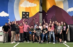
Atomica is changing the world. Working at Atomica is truly a one-of-a-kind opportunity to impact groundbreaking technology while living in paradise. Your contributions to our MEMS technology will drive innovation, solve the great problems of our time and directly impact the lives of people across the globe.
Life in Santa Barbara:
Want to live in paradise? Life in Santa Barbara is just that. Atomica is sandwiched between the beautiful Santa Ynez mountains and the pristine Central California coastline. The weather? Absolutely gorgeous. No more shoveling snow or hiding from tornadoes!
Within 5-minutes from the office, you will find rich local culture, world class schools, airport for convenient travel, festivals, and excellent options to wine and dine.
We have had employees move from all over the country and say life has never been better!
Compensation:
$90,000-$155,000
*Atomica encourages applications from candidates at all levels where pay will be based on experience.*
About Atomica:
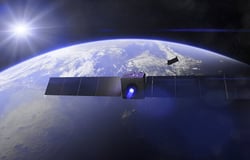
Atomica Corp. unleashes the power of Micro Electro-Mechanical Systems (MEMS) to help solve the great problems of our time. Utilizing a uniquely collaborative approach to development and manufacturing, it partners with innovative companies to deliver breakthrough MEMS-based solutions in cloud computing, autonomous vehicles, cell therapy, molecular diagnostics, genomics, 5G, the Internet of Things (IoT), and more.
Atomica is the largest MEMS foundry in the USA, serving customers from its 130,000 ft2 manufacturing campus (including a 30,000 ft2 class 100 cleanroom) in Santa Barbara, California. The company is ISO 9001 certified and ITAR registered. Its extensive experience spans the full spectrum of MEMS, including photonics, sensors, microfluidic biochips, and other micro components.
Top Skills
What We Do
Atomica Corp. unleashes the power of Micro Electro-Mechanical Systems (MEMS) to help solve the great problems of our time. Utilizing a uniquely collaborative approach to development and manufacturing, it partners with innovative companies to deliver breakthrough MEMS-based solutions in cloud computing, autonomous vehicles, cell therapy, molecular diagnostics, genomics, 5G, the Internet of Things (IoT), and more. Atomica is the largest MEMS foundry in the USA, serving customers from its 130,000 square foot manufacturing campus (with a 30,000 square foot class 100 clean room) in Santa Barbara, California. The company is ISO 9001 certified and ITAR registered. Its extensive experience spans the full spectrum of MEMS, including photonics, sensors, microfluidic biochips, and other micro components