
General Description:
The Senior Manager of Semiconductor Process Engineering in the Microfabrication Technology Laboratory (MTL) is a 2nd-level managerial position (Department Manager) responsible for managing a diverse group of approximately 50 engineers, organized into six functional areas, who maintain, improve, and develop new semiconductor processes for HRL’s broad semiconductor technology portfolio. The technologies include high-speed GaN and InP circuits, superconducting devices, MEMS-based gyroscopes, and quantum computing devices, along with other research-level devices. A key focus is moving strategic technologies from R&D to low-volume production, in keeping with HRL’s technology transition mission.
Essential Duties:
Provide engineering leadership that improves process discipline but allows for flexibility to develop new processes when appropriate, for new devices.
Maintain and improve tool/process control plans, working closely with equipment personnel.
Regularly review process control data and look for ways to improve process outcomes, advocating as needed for enhancements to process architecture, layout, and metrology.
Maintain close relationships with internal and external customers to be aware of future process needs. Establish process roadmaps for each of the six functional areas.
Work closely with the Process Integration department on “Design for Manufacturability” areas for new products, while improving process standardization for existing products.Track scrap and rework causes and establish improvement plans.
Maintain process documentation and ensure that engineers provide regular training to Production personnel.
Required Skills:
Be able to communicate effectively to both executive staff and process technicians.
An enthusiasm and talent for providing motivation, as a leader, while also demonstrating detailed, structured, management of timelines.
Thorough understanding of semiconductor process modules including photolithography, ebeam lithography, dry etch, wet etch, chemical vapor deposition (CVD), and physical vapor deposition (PVD), and atomic layer deposition (ALD).
Expertise with Statistical Process Control is required.
Familiarity with the ISO 9001 quality standard is a plus.
Six sigma green belt or higher is a plus.
An ability to multitask across functional areas and the demands of many simultaneous improvement projects is required.
Excellent interpersonal skills including the ability to lead and motivate a diverse team.
Excellent customer service skills, including clarity of communication and enthusiasm for meeting deliverables.
Required Education:
M.S. or Ph.D. plus at least 10 to 15 years of experience working in a semiconductor cleanroom environment.
At least 10 years of managing semiconductor personnel.
Physical Requirements:
Ability to work in a cleanroom environment.
Special Requirements:
U.S. citizenship/Ability to obtain and maintain a government sec
Compensation:
The base salary range for this full-time position is $182,720 - $234,168 + bonus + benefits.
Our salary ranges are determined by role, level, and location. The range displayed on each job posting reflects the minimum and maximum target for new hire salaries for the position. Within the range, individual pay is determined by work location and additional factors, including job-related skills, experience, and relevant education or training. Your recruiter can share more about the specific salary range during the hiring process. Please note that the compensation details listed reflect the base salary only, and do not include potential bonus or benefits.
What the Team is Saying


Similar Jobs
What We Do
HRL Laboratories, LLC, Malibu, California, (hrl.com) pioneers the next frontiers of physical and information science. Delivering transformative technologies in automotive, aerospace and defense, HRL advances the critical missions of its customers. As a private company owned jointly by Boeing and GM, HRL is a source of innovations that advance the state of the art in profound and far-reaching ways.
Why Work With Us
Our success is the result of our collaborative team of researchers, many of whom are the leading experts in their fields. Through their insights in support for our customers, we are finding the unique opportunities in technology.
Gallery
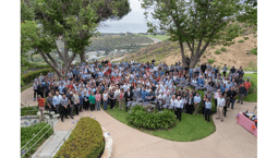


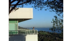

HRL Laboratories Offices
Hybrid Workspace
Employees engage in a combination of remote and on-site work.
Hybrid Policy is role specific.