Role Summary
The Senior Staff / Principal Process & Defect Engineer is responsible for driving defect reduction, process development, and cross-functional project execution across wafer fabrication operations. This role owns defect strategy, excursion response, and process improvement initiatives, while partnering with integration, equipment, and operations teams to improve yield, stability, and manufacturability.
Defect Engineering & Yield Ownership
- Own defect performance across assigned process areas (FEOL/BEOL integration loops)
- Lead defect excursion response, lot disposition (MRB / ICAR support), and root cause analysis
- Drive defect reduction strategy using Pareto, correlation, and signature mapping
- Define monitoring strategies (KLA / inspection layers) and OCAP triggers
Process Development & Optimization
- Design and execute DOE experiments and split lot analysis
- Optimize inspection strategies, recipes, and tool conditions
- Develop Best Known Methods (BKM)
- Support new process introduction and evaluate defect risks
Cross-Functional Project Leadership
- Lead multi-discipline yield and defect reduction projects
- Coordinate across process, equipment, operations, and defect teams
- Drive project execution, timelines, and technical deliverables
- Present findings and recommendations to leadership
Defect Metrology & Tool Strategy
- Own defect inspection tools (KLA, SEM)
- Develop inspection recipes and sensitivity optimization
- Ensure tool matching and data consistency
- Translate defect signatures into process actions
Manufacturing Support & Continuous Improvement
- Support fab operations and escalation response
- Improve communication and passdown structure
- Standardize defect workflows and documentation
- Identify improvements for cycle time and efficiency
Qualifications
Required:
Bachelor’s or higher in:
Electrical Engineering, Materials Science, Chemical Engineering, Physics, or related field
8+ years (Senior) or 12+ years (Principal) in:
Semiconductor manufacturing
Defect engineering, yield, or process integration
Strong background in:
Defect inspection (KLA, SEM review)
Data analysis (JMP, Python, SQL, or equivalent)
DOE and statistical analysis
Preferred:
Experience with:
Cross-functional fab leadership
Project/program management
new product development (NPD) learning cycles
Knowledge of:
SPC systems
Yield modeling and defect classification systems
*Please note that this position may require U.S. Citizenship or Permanent Residency status in the future depending on federal requirements*
What We Offer
Salary: The estimated base salary range for the position is $111,000-$154,000. The pay offered is based on many factors including, but not limited to, relevant education, job-related experience, skills and level of the position.
Benefits & Other Eligible Compensation: Includes health, dental, vision, disability and life insurance, 401(k) plan with company match, paid time off, annual bonus, and tuition reimbursement.
Polar Semiconductor is an Equal Opportunity Employer and prohibits discrimination and harassment of any kind. We are committed to the principle of equal employment opportunity for all employees and to providing employees with a work environment free of discrimination and harassment. All employment decisions are based on business needs, job requirements, and individual qualifications, without regard to race, color, religion, sex, sexual orientation, gender identity, age, national origin, disability, veteran status, or any other status protected by the laws or regulations in the locations where we operate.
About Minneapolis/St. Paul Area
Our offices and manufacturing facility are located in Bloomington, Minnesota, a suburb of Minneapolis. Living in the Minneapolis / Saint Paul area offers a strong sense of community, a vibrant arts and music scene, and abundant outdoor activities year-round. The city boasts a lower cost of living than many major metros, excellent parks and lakes, and a well-educated workforce with diverse job opportunities. Its distinct seasons bring variety, from colorful autumns to lively summers filled with festivals and waterfront activities.
Skills Required
- Bachelor's or higher in Electrical Engineering, Materials Science, Chemical Engineering, Physics, or related field
- 8+ years (Senior) or 12+ years (Principal) in semiconductor manufacturing and defect engineering, yield, or process integration
- Experience with defect inspection tools and review (KLA, SEM)
- Data analysis experience (JMP, Python, SQL, or equivalent)
- DOE and statistical analysis experience
- Cross-functional fab leadership experience
- Project or program management experience
- Experience with new product development (NPD) learning cycles
- Knowledge of SPC systems, yield modeling, and defect classification systems

What We Do
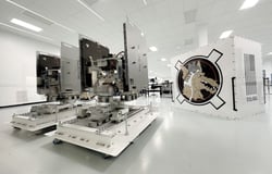
Located in Bloomington, Minnesota, Polar Semiconductor LLC has decades of experience in high-performance, automotive-grade semiconductor manufacturing. As the wafer fabrication and R&D division of Sanken Electric Company, we operate more than 310,000 square-foot facility that includes 160,000 square-feet of class-1 cleanroom space. We specialize in 200mm wafer fabrication on proprietary semiconductor technologies with most destined for use in robust automotive, commercial and industrial applications. With investments in new clean room space, state of the art equipments, and advanced silicon technologies, Polar continues to enhance its manufacturing competitiveness. Polar is ISO 14001 and IATF 16949 certified