Snap Inc is a technology company. We believe the camera presents the greatest opportunity to improve the way people live and communicate. Snap contributes to human progress by empowering people to express themselves, live in the moment, learn about the world, and have fun together.
The Company operates Snapchat, a visual messaging app that enhances your relationships with friends, family, and the world, and Specs Inc., a wholly-owned subsidiary dedicated to making computing more human, in addition to Bitmoji, Saturn, and other digital services.
The Spectacles team is pushing the boundaries of technology to bring people closer together in the real world. Our fifth-generation Spectacles, powered by Snap OS, showcase how standalone, see-through AR glasses make playing, learning, and working better together.
Snap’s camera supports real friendships through visual communication, self expression and storytelling. Moving forward, our camera will play a transformative role in how people experience the world around them, combining what they see in the real world, with all that’s available to them in the digital world.
We’re looking for a Packaging Process Engineer to join our team at Snap Inc!
What You’ll Do:This role will serve as the technical process owner for backend packaging and continuity testing tool, supporting our advanced displays from prototyping through production. As an engineer you would drive process development, yield, and manufacturability on our microdisplay production line.
Additionally you will:
Own and optimize a backend packaging process for LCOS advanced displays, from early development through high-volume manufacturing, ensuring stable, high-yield output.
Act as the primary technical interface for equipment, materials, and manufacturing partners, overseeing tool qualification, process capability, build readiness, and issue resolution.
Develop, qualify, and sustain assembly and packaging recipes, control plans, and SPC systems, driving continuous improvement in CD/overlay, defectivity, yields, and reliability.
Lead structured problem solving (DOEs, FMEA, root cause analysis, corrective actions) for yield excursions, line stops, and parametric drifts.
Partner with cross-functional teams to define capacity models and WIP/uptime strategies.
Hands-on experience with automated packaging equipment, including recipe setup, tuning, and troubleshooting.
Proven ability to function as a module owner in a high-volume fab or OSAT environment, balancing NPI design transfer activities and roadmap work.
Exceptional problem solver with a structured, solution focused approach, leveraging advanced statistical tools to improve yield and stability in packaging.
Comfortable working in an ISO 5 cleanroom environment and enforcing best practices in contamination control, safety, and EHS compliance.
BS degree in Electrical Engineering, Materials Science, Mechanical Engineering, or a related technical field
7+ years of experience as a process or packaging engineer in microfabrication fabs.
Direct experience designing and optimizing automated production equipment for semiconductors or displays
Direct experience in final test for semiconductor or display packages.
Demonstrated track record of improving yield and process stability through structured experimentation (DOE), SPC, and cross-functional problem solving.
Experience planning and executing process transfers from R&D to production lines.
International travel between Taiwan, U.S., and supplier sites (up to ~10%).
10+ years of experience in process engineering and backend packaging.
Ownership of module performance and direct collaboration with applications engineers.
Excellent problem solver with a foundation in Six Sigma.
Experience with automated optical assembly and test equipment.
Experience developing and sustaining wire bonding processes (materials, bond parameters, loop profiles, pad design interfaces) for high‑density LOCS packages.
Strong expertise in backend assembly processes for advanced displays, including die attach, marking, and final packing.
If you have a disability or special need that requires accommodation, please don’t be shy and provide us some information.
"Default Together" Policy at Snap: At Snap Inc. we believe that being together in person helps us build our culture faster, reinforce our values, and serve our community, customers and partners better through dynamic collaboration. To reflect this, we practice a “default together” approach and expect our team members to work in an office 4+ days per week.
At Snap, we believe that having a team of diverse backgrounds and voices working together will enable us to create innovative products that improve the way people live and communicate. Snap is proud to be an equal opportunity employer, and committed to providing employment opportunities regardless of race, religious creed, color, national origin, ancestry, physical disability, mental disability, medical condition, genetic information, marital status, sex, gender, gender identity, gender expression, pregnancy, childbirth and breastfeeding, age, sexual orientation, military or veteran status, or any other protected classification, in accordance with applicable federal, state, and local laws. EOE, including disability/vets.
We are an Equal Opportunity Employer and will consider qualified applicants with criminal histories in a manner consistent with applicable law (by example, the requirements of the San Francisco Fair Chance Ordinance and the Los Angeles Fair Chance Initiative for Hiring, where applicable).
Our Benefits: Snap Inc. is its own community, so we’ve got your back! We do our best to make sure you and your loved ones have everything you need to be happy and healthy, on your own terms. Our benefits are built around your needs and include paid parental leave, comprehensive medical coverage, emotional and mental health support programs, and compensation packages that let you share in Snap’s long-term success!
Compensation
In the United States, work locations are assigned a pay zone which determines the salary range for the position. The successful candidate’s starting pay will be determined based on job-related skills, experience, qualifications, work location, and market conditions. The starting pay may be negotiable within the salary range for the position. These pay zones may be modified in the future.
Zone A (CA, WA, NYC):
The base salary range for this position is $142,000-$214,000 annually.
Zone B:
The base salary range for this position is $135,000-$203,000 annually.Zone C:
The base salary range for this position is $121,000-$182,000 annually.This position is eligible for equity in the form of RSUs.Skills Required
- BS degree in Electrical Engineering, Materials Science, Mechanical Engineering, or related field
- 7+ years of experience as a process or packaging engineer in microfabrication fabs
- Direct experience designing and optimizing automated production equipment for semiconductors or displays
- Direct experience in final test for semiconductor or display packages
- Demonstrated track record of improving yield and process stability through structured experimentation (DOE), SPC, and cross-functional problem solving
- Experience planning and executing process transfers from R&D to production lines
- International travel between Taiwan, U.S., and supplier sites (up to ~10%)
What the Team is Saying


.png)


.png)


Snap Inc. Compensation & Benefits Highlights
-
Parental & Family Support — Parental leave, family‑building benefits, caregiver assistance, and backup child care are described as extensive and well‑structured. Return‑to‑work support and lactation resources add practical help for families.
-
Healthcare Strength — Medical, dental, and vision coverage are broad, with mental‑health sessions, One Medical access, wellness reimbursements, and virtual physical therapy included. These offerings indicate a comprehensive approach to health and well‑being.
-
Retirement Support — A 401(k) with employer matching and an after‑tax “mega backdoor” option supports flexible, higher‑ceiling savings. HSAs/FSAs and related financial resources further strengthen overall financial wellness.
Snap Inc. Insights
What We Do
We contribute to human progress by empowering people to express themselves, live in the moment, learn about the world, and have fun together.
Gallery

Snap Inc. Teams


Snap Inc. Offices
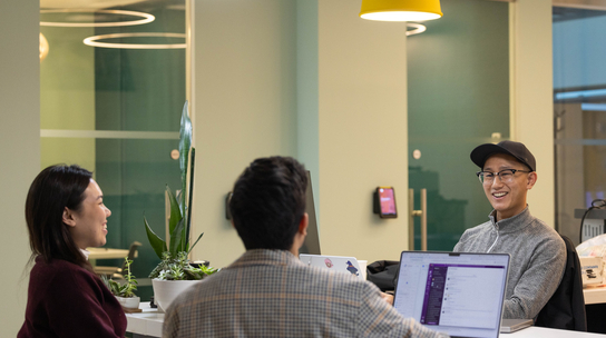
Hybrid Workspace
Employees engage in a combination of remote and on-site work.
Our “default together” approach is an 80/20 model where we are asking team members to spend 80% of the time, on average, in the office, with the remaining 20% of the time spent remote.