The Role
Contribute to photonic packaging and testing: iterate interface designs, characterize and qualify high-frequency solutions, document results, and collaborate with design and process teams. Report findings to Swiss PIC experts.
Summary Generated by Built In
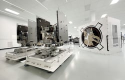
Swiss Photonics Integration Center (Swiss PIC) provides precision assembly and characterization solutions for Swiss industry, especially start-ups and SMEs. High-speed systems are widely demanded in optical communications, sensing, quantum computing, etc. and testing and qualification are crucial steps to verify the products performance. The center, which is located in the Switzerland Innovation, Park InnovAARE, next to the Paul Scherrer Institute (PSI), is investing in qualified industrialized processes, clean environmentally controlled fabs, high-tech machinery, and has built up a full production line for optical and electrical precision assembly.
The Opportunity: We are seeking an intern to contribute to photonic packaging and testing services for a minimum duration of 4 months. If you are experienced in Optical and/or RF or characterization and packaging or familiar with the related lab equipment, you are highly encouraged to apply, otherwise an openness to learn and readiness to tackle the task at hand while learning from our experienced specialists is a must. If this is of your interest, send your application to join our international and dynamic team of experts dedicated to pushing the boundaries of what is possible in photonics and shape the future of technologies within communication, computing, quantum and beyond.
Tasks
* Systematic test and iteration on interface designs, using state-of-the-art tools and methodologies to extract best designs for high-frequency interfacing
* Characterize and qualify the developed solutions and technical documentation of the results
* Closely collaborate with the design and process engineering teams to develop and improve solutions that meet performance requirements and manufacturing constraints.
* Clear and timely reporting to Swiss PIC experts
Requirements
* Bachelor, master, or PhD in Electrical Engineering, Physics, or a related field.
* Hands on experience with optical or RF characterization equipment such as tunable lasers, OSAs, power meters, vector network analyzers (VNAs) or Lightwave component analyzers (LCAs) is a plus
* Experience with chip facet polishing tools is a plus.
* Technical documentation skills and systematic reporting. Self-motivated and able to work independently.
* Strong analytical and problem-solving skills, with the ability to troubleshoot complex issues and propose effective solutions.
* Experience with semiconductor packaging, microelectronics or micromechanics is a plus.
* Solid communication skills in English required.
Benefits
* Opportunity to work on groundbreaking technology at the forefront of the industry, shaping the future of communication and computing.
* International, Collaborative and inclusive team culture that values creativity, diversity, and continuous learning.
* Personal responsibility in your job and the chance to grow with us.
* Our passion to bring PICs to every day’s life.
Employment rate: 60% or by arrangement, Place of work: Villigen, Switzerland Start date: from June 2026 Duration: at least 4 months
How to Apply: We look forward to receiving your application, including:
* Your CV
* (Optional) A statement of interest relating the position to your skills
* (Optional) Grades or work certificates, or references if available
Applications will be reviewed on a rolling basis
Skills Required
- Bachelor, Master, or PhD in Electrical Engineering, Physics, or a related field.
- Hands on experience with optical or RF characterization equipment such as tunable lasers, OSAs, power meters, VNAs or LCAs.
- Experience with chip facet polishing tools.
- Technical documentation skills and systematic reporting.
- Self-motivated and able to work independently.
- Strong analytical and problem-solving skills, ability to troubleshoot complex issues and propose solutions.
- Experience with semiconductor packaging, microelectronics or micromechanics.
- Solid communication skills in English.
Am I A Good Fit?
Get Personalized Job Insights.
Our AI-powered fit analysis compares your resume with a job listing so you know if your skills & experience align.
Success! Refresh the page to see how your skills align with this role.
The Company
What We Do
The Swiss Photonics Integration Center (Swiss PIC) provides advanced packaging and integration services for photonic microchips, bridging the gap between innovation and market-ready modules. They offer precision assembly, testing, and qualification for photonic systems, supporting start-ups and SMEs in launching their products through high-precision machinery and industrialized processes, facilitating the transition from first concept to scalable product.